


Experimental Physics of Matter: Optical Spectroscopy
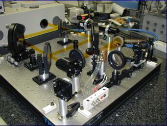
The laboratories are equipped for optical characterization with a number of different techniques and broad spectral range (from far infrared to vacuum ultraviolet). Beyond the most common measurements based on reflectance, transmittance, absorbance, photoluminescence, spectroscopic ellipsometry, systems and set-ups have been implemented to perform interferometric measurements or modulation spectroscopy techniques (such as photo- ,thermo- and electro-reflectance, photoinduced absorption), both spatially (with micro-focusing systems) and temporally (on nanosecond resolution time-scale) resolved. These techniques allow the study and characterization of vibrational and electronic properties of various bulk and nanostructured materials. A further advanced structural characterization is performed by means of atomic force microscopy (AFM). The figure to the left shows a Mach-Zehnder interferometer coupled to a Fourier-transform spectrometer.
The main research lines are related to studies on bulk semiconductors and semiconductor nanostructures, especially binary III-V compounds or Silicon/Germanium, but also metal nanoparticles (e.g. Gallium). More recently, an activity on polymeric and conjugate polymeric semiconductors has started, with emphasis on optical excitations and charge carrier dynamics. Applications of these materials (both semiconductors and polymers) are in the fields of microelectronics, optoelectronics, and photovoltaics. A major part of the research activity is related to the experimental investigation of photonic crystals, i.e. systems with a periodic dielectric constant in one, two, or three dimensions: such systems are particularly interesting for a great variety of physical phenomena and they are promising for applications to optoelectronics and optical communication, lasers, integrated photonics and photovoltaic energy conversion.
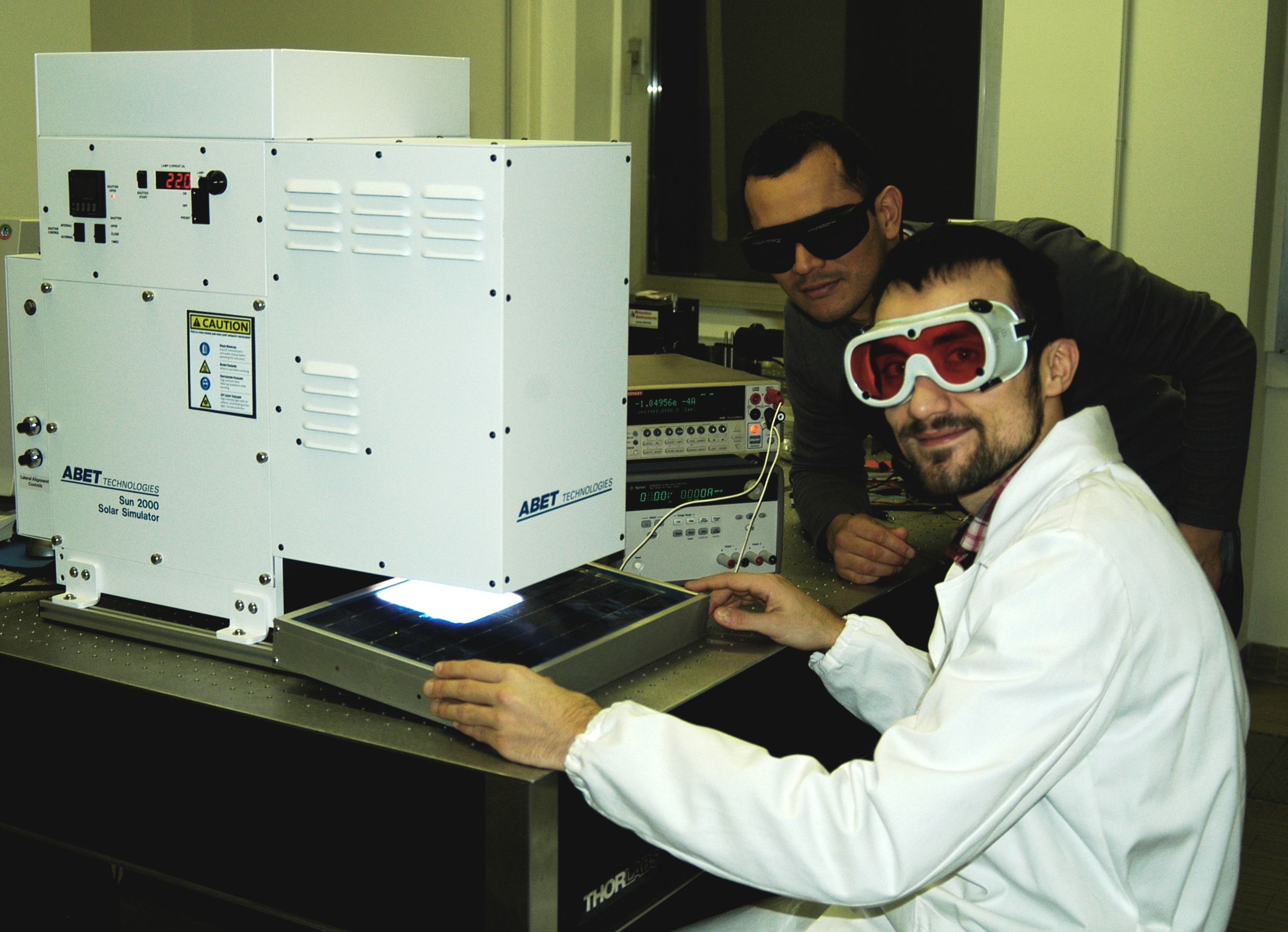
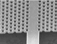
The investigated structures include photonic crystal waveguides and nanocavities in Silicon and III-V semiconductors for all-optical switching and enhanced light emission, but also 3D structures like direct and inverse opals. Recent developments concern ultra-low power silicon photonics as well as quantum and nonlinear photonics. Moreover, nanostructured metal surfaces are of great interest, as well as hybrid metal/dielectric systems with plasmonic excitations, with applications to the development of highly-sensitive optical bio-sensors. A highly interesting activity concerns photovoltaic cells made of semiconductors and of organic materials, that are studied by means of CW and time-resolved spectroscopic techniques, as well as with electro-optical characterizations with solar simulator (see figure to the left).
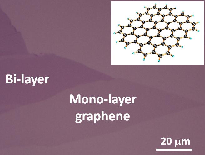
Other investigated systems are graphene and carbon based material. Among them, graphene is stiff, light, nearly transparent and an excellent conductor of heat and electricity. The optical, vibrational and electronic properties of graphene and carbon based materials make them attractive for several applications. Among them we have flexible electronics, bio-physics and energy science and technology. Moreover electrons in graphene obey to a Dirac-like equation so that the experiments allow investigating experimentally many relativistic quantum phenomena.
Staff: M. Galli, M. Geddo, F. Marabelli, M. Patrini (photonics and nanostructures), V. Bellani (graphene and carbon nanostructures)