Modulation Spectroscopy Laboratory
at the Physics Department , University of Pavia

LSM director: Mario Geddo
The research carried out in the Laboratory of Modulation Spectroscopy mainly concerns the study of semiconductor systems (bulk, thin films and heterostructures in reduced dimensionality) manufactured with epitaxial growth techniques (MBE).
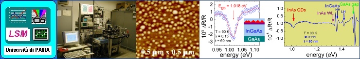
The modulation techniques available are Photoreflectance, Thermoreflectance and Electroreflectance. These non-destructive diagnostic methods are particularly effective and reliable in the characterization of multi-layer systems and nanostructures that, in itself interesting from a fundamental point of view, have performed in the last years a growing growing importance for their applications in microelectronics and optoelectronics. Just think of how the fascinating field of Quantum Dots (typically single crystal InAs self-aggregates in a GaAs matrix) has attracted increasing research efforts aimed at nanoscale optoelectronic devices such as lasers and photo detectors made with quantum dots (QDs) technology. At the same time the behavior of "artificial atom" exhibited by the nanocrystals has been an excellent test to study phenomena related to quantum confinement in Condensed Matter Physics.
The semiconductor systems studied and/or in the course of analysis are:
- III-V alloys and quantum wells (GaAs-AlGaAs, InGaP-GaP, InGaAs-GaAs, GaSb-AlGaSb)
- InAs QDs self-aggregated in matrix of GaAs, InGaAs, AlGaAs
- thin films and quantum wells of dilute nitrides (InGaAsN-GaAs, GaAsN-GaAs, GaPN-GaP, InGaN-GaN)
In many cases, the research was carried out as part of the National Targeted Projects also producing interesting application outcomes. It cites, for example:
- The study of the optical properties of nanostructures (InAs/InGaAs QDs) as a function of strain and composition of the confinement layers allowed to tune the wavelength of the characteristic emission of the dots to 1.31 and 1.55 microns, i.e. in correspondence to spectral windows of specific interest in fiber optic communications.
- The study of the optical properties of diluted nitrides irradiated with hydrogen in function of the implanted dose and the initial concentration of nitrogen has allowed us to demonstrate the possibility of obtaining, with a single process, the simultaneous confinement of carriers and photons in the plane of growth of GaAsN , with important consequences for the realization of optoelectronic couplers and waveguides in planar technology based on GaAs.
Latest news:
dilute nitrides
- May 2019 - A study on the selection rules of the GaAs-like LO Raman modes in hydrogenated GaAsN layers highlighting interesting suggestions for strain modulation in the growth plane is presented in "Strain related relaxation of the GaAs-like Raman mode selection rules in hydrogenated GaAsN layers"
----
- November 2019 - A review of the analytical and experimental procedure devised and applied in recent years (since 2011) to study the evolution of strain and its link with the formation of N-H complexes in hydrogenated diluted nitrides, is presented in the paper "Micro-Raman Mapping of the Strain Field in GaAsN/GaAsN:H Planar Heterostructures: A Brief Review and Recent Evolution"